Connectors tour
JP150PCB 1.3PCB 1.4Jan PřibyslavskýThis page does not apply to the product or PCB revision chosen in the header.
On this page you find every connector and indicator of the board under the name printed next to it, what it is for, which board revision has it, and the link to its pinout. The outline (140 × 105 mm) and the mounting holes are the same on both revisions (Mechanical); PCB 1.4 changed the pin order of a few headers, added the 12 V trigger and a second I2S output, and has no DIP switch.
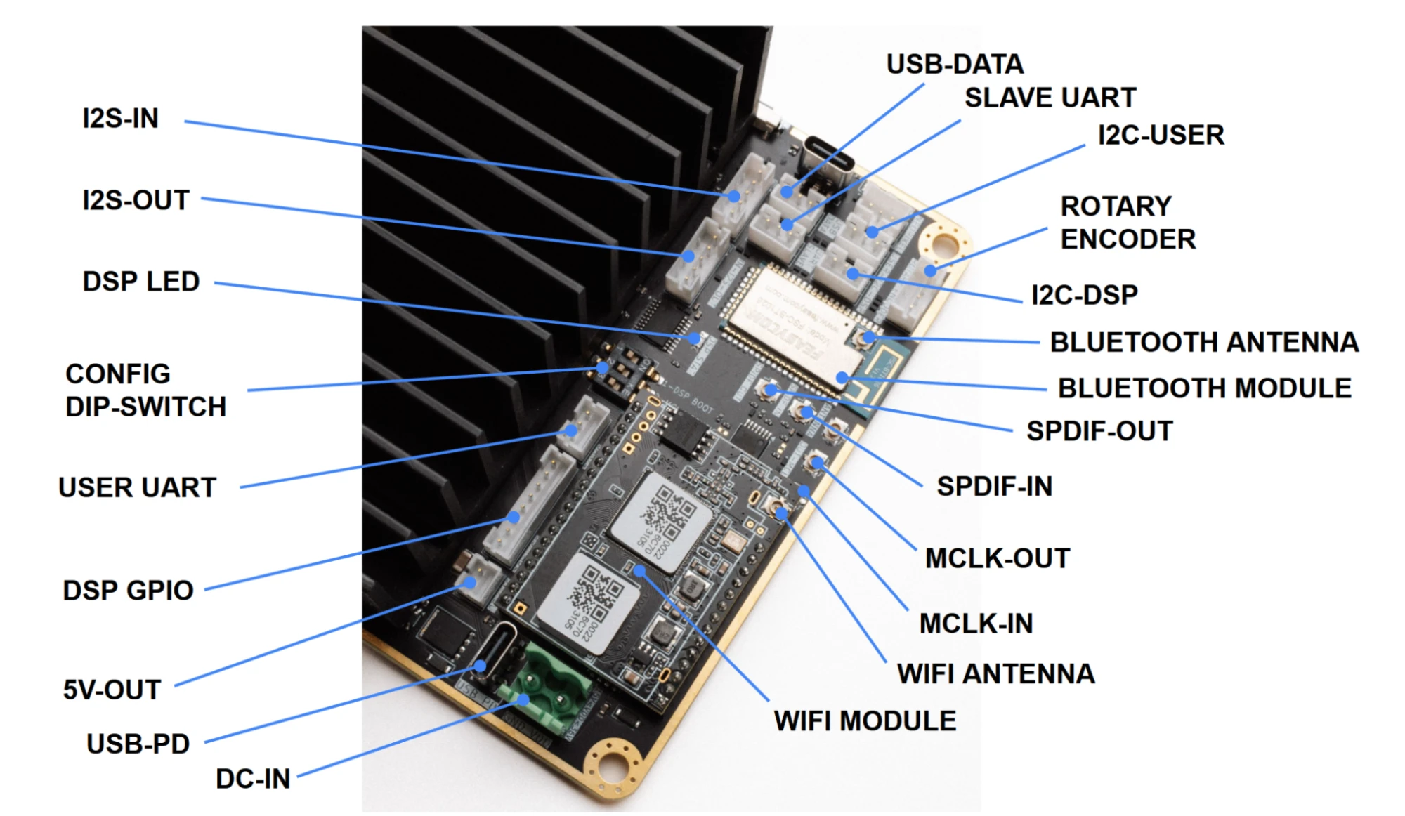
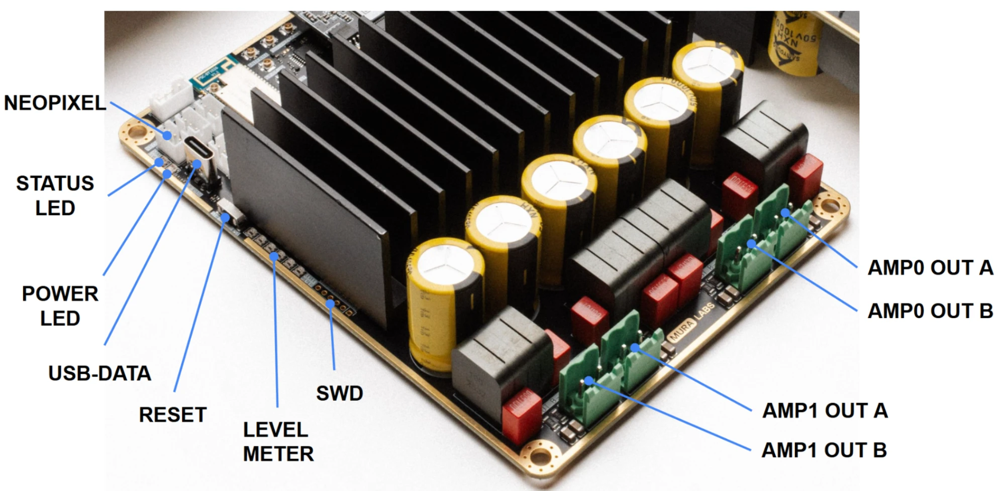
To be added
Photographs of PCB 1.4 with its connectors labelled; the positions differ slightly from PCB 1.3.
Power and speakers
| Label | What it is | Boards | Pinout |
|---|---|---|---|
| POWER IN | DC supply, 15 to 36 V, screw terminal; pin 1 GND, pin 2 positive | 1.3, 1.4 | Power inputs |
| USB C PD | USB Power Delivery supply up to 100 W, power only | 1.3, 1.4 | Power inputs |
| AMP0 OUT A, AMP0 OUT B, AMP1 OUT A, AMP1 OUT B | The four speaker outputs of the two power stages, + and − marked | 1.3, 1.4 | Speaker outputs, Configuration |
| 5V PSU | 5 V output for accessories; the pin order differs between the revisions | 1.3, 1.4 | 5 V output |
Audio in and out
| Label | What it is | Boards | Pinout |
|---|---|---|---|
| I2S INPUT, I2S OUTPUT | Digital audio in and out, 5-pin JST PH; the pin order differs between the revisions | 1.3, 1.4 | I2S input and output |
| I2S OUTPUT AUX | A second I2S output from the DSP's serial port 1 | 1.4 | I2S input and output |
| SPDIF IN, SPDIF OUT | S/PDIF digital audio in and out on coaxial connectors | 1.3, 1.4 | Coaxial connectors |
| MCLK-IN, MCLK-OUT | External master clock in (not used by the firmware) and the DSP clock out | 1.3, 1.4 | Coaxial connectors |
| BLUETOOTH ANTENNA, WIFI ANTENNA | Antenna connectors; the Wi-Fi antenna is mandatory for Wi-Fi operation | 1.3, 1.4 | Coaxial connectors |
Control and data
| Label | What it is | Boards | Pinout |
|---|---|---|---|
| USB DATA (USB-C connector and 3-pin header) | USB audio and the control interface as a virtual COM port; use one of the two | 1.3, 1.4 | USB data |
| UART1 | The control interface over UART, 115200 baud 8N1; the pin order differs between the revisions | 1.3, 1.4 | User UART |
| UART SLAVE | For connecting another module | 1.3, 1.4 | Slave UART |
| ROTARY ENCODER | The volume encoder with its push button | 1.3, 1.4 | Encoder |
| 12V TRIGGER | Trigger input from another device or a panel button | 1.4 | 12 V trigger, Operation |
| NEOPIXEL | An external addressable LED chain on the indicators' data line | 1.3, 1.4 | Neopixel |
DSP and service
| Label | What it is | Boards | Pinout |
|---|---|---|---|
| I2C-DSP | The SigmaStudio USBi programmer | 1.3, 1.4 | DSP I2C, Quick start |
| DSP GPIO (1.4), I2C-USER (1.3) | On PCB 1.4 two multipurpose pins of the DSP; on PCB 1.3 a reserved I2C bus | 1.3, 1.4 | User I2C and DSP GPIO |
| DSP ADC | Auxiliary ADC and GPIO inputs of the DSP, 8 pins; the pin order is mirrored on PCB 1.4 | 1.3, 1.4 | DSP GPIO / ADC inputs |
| STM PROGRAMMER | The SWD debug port, closed on production modules | 1.3, 1.4 | SWD |
| DIP switch | DSP self boot, master clock and MCU boot selection | 1.3 | Configuration |
| STM BOOT | Solder jumper for the MCU boot pin, open in normal use | 1.4 | Configuration |
Indicators
The power LED, the status LED, the DSP LED and the six-LED level meter sit on both revisions; PCB 1.4 adds the CLIP and FAULT LEDs of each power stage, the Bluetooth module's LEDs and the USB-C supply LED. What each shows is on Indicators and LEDs.