Connectors and pinouts
JP150PCB 1.3PCB 1.4Jan PřibyslavskýThis page does not apply to the product or PCB revision chosen in the header.
On this page you find the pinout of every connector, under the name printed next to it on the board. Pick your board revision once, in the tabs below or in the filter at the top of the page; every tab on the site follows the choice. Pin 1 is the pin marked on the board next to each connector.
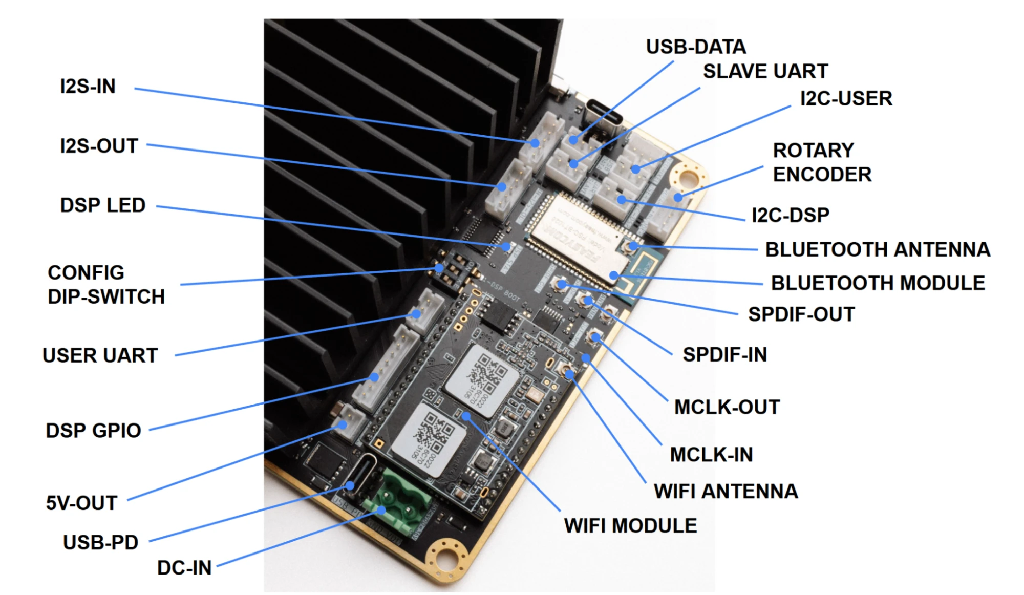
To be added
Drawings of the connector positions of PCB 1.3 and PCB 1.4, which differ slightly.
Check the revision before you make a cable
PCB 1.4 moved the pins of the I2S, UART1, DSP GPIO and 5 V connectors. A cable made for a 1.3
board fits a 1.4 board mechanically, with the signals in other positions. Read the revision
from the silkscreen, or ask the module: SYS:BOARD:TYPE? answers JP150-1.3 or JP150-1.4.
Power inputs
DC-IN (POWER IN). Screw terminal, 15 to 36 V DC: pin 1 GND, pin 2 positive. The module has reverse-polarity protection and soft-start inrush limiting. Keep the supply leads short and low-impedance; do not exceed 36 V (see Specifications).
USB-PD (USB C PD). USB Power Delivery input up to 100 W, power only. On PCB 1.4 a green LED
next to the connector shows that a USB-C source is present, and the firmware reports it
(SYS:POWER:USBC?).
Speaker outputs
Four screw-terminal outputs for the two TAS3251 power stages: AMP0 OUT A, AMP0 OUT B, AMP1 OUT A, AMP1 OUT B, each with its + and − pin marked. With the default DSP program, OUT A carries the left and OUT B the right channel of each power stage; an own DSP program can route the channels differently. The BTL and PBTL bridging options are on Configuration.
I2S input and output
JST PH, 5 pins. Two connectors as before (I2S INPUT, I2S OUTPUT) plus the auxiliary output (I2S OUTPUT AUX) on the DSP's serial output port 1. since 26.10.1
| Pin | I2S INPUT | I2S OUTPUT | I2S OUTPUT AUX |
|---|---|---|---|
| 1 | GND | GND | GND |
| 2 | BCLK | BCLK | BCLK 1 |
| 3 | GND | GND | GND |
| 4 | LRCLK | LRCLK | LRCLK 1 |
| 5 | DATA IN | DATA OUT | DATA OUT 1 |
JST PH, 5 pins. Two connectors (I2S INPUT, I2S OUTPUT); PCB 1.3 has no auxiliary output.
| Pin | I2S INPUT | I2S OUTPUT |
|---|---|---|
| 1 | DATA IN | DATA OUT |
| 2 | GND | GND |
| 3 | BCLK | BCLK |
| 4 | GND | GND |
| 5 | LRCLK | LRCLK |
Use shielded cable for the best signal integrity. Digital audio up to 96 kHz / 32 bit, I2S and TDM modes, as configured in the DSP program.
User UART (UART1)
| Pin | Signal | Description |
|---|---|---|
| 1 | GND | Ground reference |
| 2 | TX | UART transmit from the module |
| 3 | RX | UART receive into the module, 5 V tolerant |
| Pin | Signal | Description |
|---|---|---|
| 1 | RX | UART receive into the module, 5 V tolerant |
| 2 | TX | UART transmit from the module |
| 3 | GND | Ground reference |
115200 bit/s, 8 data bits, no parity, 1 stop bit, 3.3 V logic. Connect the module to a host with a common ground and crossed lines (host TX to module RX). The same command set is available on the USB virtual COM port; see Control interface.
Slave UART (UART SLAVE)
JST PH, 3 pins, the same on both revisions: pin 1 TX (from the module), pin 2 RX, pin 3 GND. For connecting another module.
DSP I2C (I2C-DSP)
JST PH, 3 pins, the same on both revisions: pin 1 SDA, pin 2 SCL, pin 3 GND. The connector for the SigmaStudio USBi programmer.
A bus the DSP has to itself (the module's own control bus for the DSP, 400 kHz). The power stages, the temperature sensor, the settings memory and the supply monitor are on another bus. The programmer coexistence rules still apply: a connected USBi suspends the module's own DSP traffic.
The module's shared system bus: the DSP, both power stages, the settings memory and the temperature sensor share it. A SigmaStudio session therefore shares the bus with the amplifier control, which the firmware arbitrates (programmer coexistence). Never use SigmaStudio's "Write Latest Compilation USB" on PCB 1.3: it writes to I2C address 0xA0, where the module's settings memory sits.
User I2C and DSP GPIO
On PCB 1.4 the connector carries two multipurpose pins of the ADAU1452 (silkscreen DSP GPIO): pin 1 MP6, pin 2 MP7, pin 3 GND. MP7 also drives the DSP status LED. Their function is defined by the DSP program; the firmware does not use them.
Reserved for future firmware (silkscreen I2C-USER): pin 1 SDA, pin 2 SCL, pin 3 GND, on a separate I2C bus of the MCU. Not used by the current firmware.
DSP GPIO / ADC inputs (DSP ADC)
Auxiliary ADC and GPIO inputs of the ADAU1452, JST PH, 8 pins.
| Pin | Signal |
|---|---|
| 1 | GND |
| 2 | ADC5 |
| 3 | ADC4 |
| 4 | ADC3 |
| 5 | ADC2 |
| 6 | ADC1 |
| 7 | ADC0 |
| 8 | 3V3 |
| Pin | Signal |
|---|---|
| 1 | 3V3 |
| 2 | ADC0 |
| 3 | ADC1 |
| 4 | ADC2 |
| 5 | ADC3 |
| 6 | ADC4 |
| 7 | ADC5 |
| 8 | GND |
Encoder (ROTARY ENCODER)
JST PH, 4 pins, the same on both revisions.
| Pin | Signal | Description |
|---|---|---|
| 1 | ENC_A | Quadrature signal A |
| 2 | ENC_SW | Encoder push button |
| 3 | ENC_B | Quadrature signal B |
| 4 | GND | Ground reference |
Rotate to change the volume, press to cycle the inputs. Holding the button while switching the module on enters the bootloader's update mode (Recovery). The encoder is optional; the module is fully controllable over UART and USB.
12 V trigger (12V TRIGGER)
PCB 1.4 only
JST PH, 2 pins: pin 1 trigger input, pin 2 GND. A 3.3 V to 12 V signal reads as active; the input has a series resistor and a 3.3 V clamp. What the module does with it is set by the trigger mode, see 12 V trigger. since 26.10.1
5 V output (5V PSU)
JST PH, 2 pins. 5 V from the module's own regulator for an external control board; switched off in standby.
| Pin | Signal |
|---|---|
| 1 | +5 V |
| 2 | GND |
| Pin | Signal |
|---|---|
| 1 | GND |
| 2 | +5 V |
USB data (USB DATA)
Use either the USB-C receptacle or the 3-pin JST header, both labelled USB DATA, for USB data. The module
enumerates as one composite device: USB Audio and a virtual COM port carrying the control command
set. From firmware 26.10.1 the device identifies as 16D0:15B8 ("MURA LABS JP150"); the bootloader's
update mode as 16D0:15B7. Firmware 26.8.0 and earlier identified as 0483:5741.
| Pin (3-pin header) | Signal |
|---|---|
| 1 | USB D− |
| 2 | USB D+ |
| 3 | GND |
Neopixel (NEOPIXEL)
JST PH, 3 pins, the same on both revisions: pin 1 GND, pin 2 DATA, pin 3 3V3 OUT. Reserved for an external addressable LED chain; the on-board indicators are on the same data line.
Coaxial (U.FL) connectors
| Connector | Function |
|---|---|
| MCLK-IN | External master clock input. Not used by the current firmware (the module runs from its internal clock). |
| MCLK-OUT | DSP clock output (buffered on PCB 1.4). |
| SPDIF IN, SPDIF OUT | S/PDIF digital audio in and out. |
| BLUETOOTH ANTENNA | Optional external antenna; without it the module's own antenna is used. |
| WIFI ANTENNA | External antenna, mandatory for Wi-Fi operation. |
SWD (STM PROGRAMMER)
Pin header, 2.00 mm: 1 3V3, 2 SWCLK, 3 GND, 4 SWDIO, 5 NRST, 6 SWO. Development use. On production modules the debug port is closed (read-out protection level 2).